Chapter 14: Semiconductor Electronics: Materials, Devices and Simple Circuits
For the first half of the twentieth century, almost every radio, telephone exchange, and early computer ran on vacuum tubes — glass bulbs the size of a small lamp, glowing hot inside, drawing large amounts of power, and burning out far too often. A single early computer could contain thousands of them, and keeping them all working was a daily battle.
In the late 1940s, a small team of physicists at Bell Laboratories in the United States — John Bardeen, Walter Brattain, and William Shockley — set out to build a device that could do the job of a vacuum tube using nothing but a solid piece of crystal. In 1947 they succeeded. Pressing fine metal points onto a small slab of germanium, they made the first working transistor: a device with no glowing filament, no vacuum, and no fragile glass, that could still control and amplify an electric current. The three later shared the Nobel Prize for this work.
That small crystal changed the world. The bulky, hot, power-hungry tube was replaced by a tiny, cool, reliable solid-state device. Every phone, laptop, and memory chip you use today is a direct descendant of that experiment. But to understand how a mere piece of crystal can control electric current, we must first understand what makes a material a semiconductor.
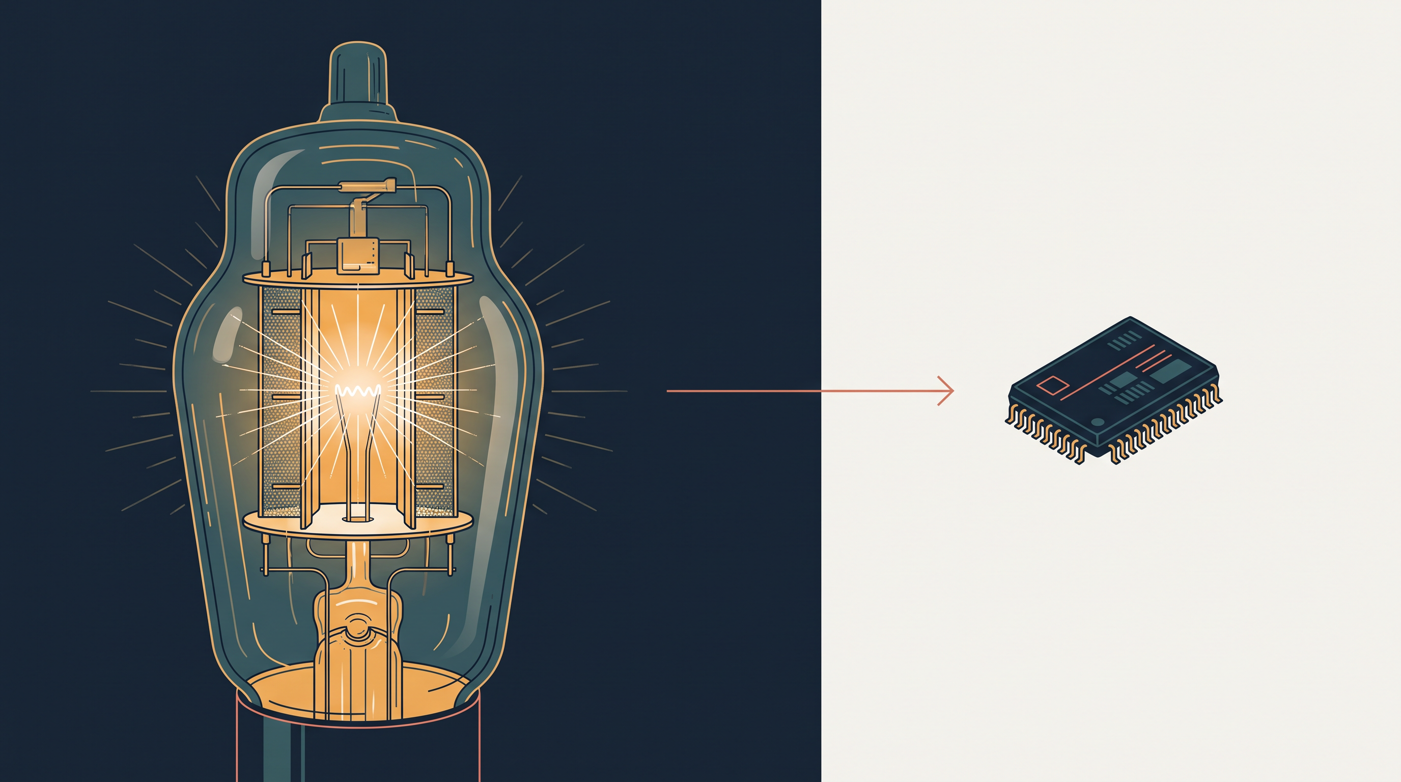
Fig. 14.0 – Vacuum tube and modern semiconductor chip.
By the end of this chapter, you will be able to answer each of these questions.
14.1 Introduction
Every electronic circuit — inside a radio, a computer, or a mobile phone — is built from devices in which the flow of electrons can be controlled. If we can decide how many electrons flow and in which direction they flow, we can build switches, amplifiers, detectors, and much more. Devices that give us this controlled flow of electrons are therefore the basic building blocks of all electronic circuits.
Before the transistor came into use around 1948, most of these devices were vacuum tubes, also called valves. To understand why semiconductors later replaced them, it helps to first see how these tubes worked and what their limitations were.
The simplest vacuum tube is the vacuum diode, which has two electrodes. Here an electrode simply means a conductor through which electrons enter or leave the device. The two electrodes of a diode are the anode (often called the plate) and the cathode. A triode has three electrodes — cathode, plate, and a grid — while the tetrode and pentode have four and five electrodes respectively.
Inside a vacuum tube, the electrons are supplied by a heated cathode. Heating a metal gives some of its electrons enough energy to escape from its surface, releasing free electrons into the space around it. The controlled flow of these electrons is then obtained by varying the voltage applied between the different electrodes — changing the voltage changes how easily electrons move from one electrode to another.
A vacuum is required in the space between the electrodes. If air were present, the moving electrons would keep colliding with air molecules and lose their energy before reaching the other electrode, so the device would not work properly.
An important feature of these tubes is that electrons can flow only from the cathode to the anode, that is, in one direction only. Because they allow current in one direction and block it in the other — just as a mechanical valve allows fluid to pass one way — such devices are generally referred to as valves.
These vacuum tube devices had several serious drawbacks. They were bulky, consumed a lot of power, generally needed high operating voltages (of the order of 100 V), and had a limited working life together with low reliability. A machine using thousands of such tubes was large, hot, and prone to frequent failures.
The seed for modern solid-state semiconductor electronics was sown in the 1930s. It was realised that certain solid-state semiconductors, and the junctions formed between them, offer the possibility of controlling both the number and the direction of flow of charge carriers through them. Even simple, gentle excitations such as light, heat, or a small applied voltage can change the number of mobile charges inside a semiconductor. This sensitivity is exactly what makes them so useful for building controllable devices.
The crucial difference is where the charge carriers come from and where they move. In a semiconductor device, the supply and the flow of charge carriers take place within the solid itself. In the older vacuum tubes, the mobile electrons had to be produced by a heated cathode and then made to travel across an evacuated space. A semiconductor device therefore needs no external heating and no large evacuated region.
Because of this, semiconductor devices are small in size, consume low power, operate at low voltages, and have long life and high reliability — precisely the advantages the fragile, power-hungry vacuum tube lacked. This is why a tiny, cool, solid crystal was able to take over the job of the bulky, glowing tube.
The advantages of solid-state electronics are visible even in everyday displays. The Cathode Ray Tubes (CRT) once used in televisions and computer monitors work on the principle of vacuum tubes, but they have largely been replaced by Liquid Crystal Display (LCD) monitors backed by solid-state electronics, which are lighter, thinner, and far more power-efficient.
Interestingly, semiconductors were put to practical use even before their behaviour was fully understood. Long before the physics was worked out, a naturally occurring crystal of galena (lead sulphide, PbS), with a fine metal point contact touching it, was used as a detector of radio waves in early radio receivers.
In the sections that follow, we will first introduce the basic concepts of semiconductor physics. We will then discuss some important semiconductor devices, such as the junction diode (a two-electrode device) and the bipolar junction transistor (a three-electrode device), and describe a few circuits that illustrate their applications.
14.2 Classification of Metals, Conductors and Semiconductors
Solids differ enormously in how easily they let electric current pass through them. A copper wire conducts almost effortlessly, dry glass hardly conducts at all, and silicon sits somewhere in between. We can classify solids in two different but related ways: first by directly comparing how well they conduct, and second by looking at the arrangement of allowed electron energies inside them.
On the basis of conductivity
The natural quantity to compare is electrical conductivity (\(\sigma\)), which measures how easily a material allows current to flow, or equivalently its resistivity (\(\rho\)), which measures how strongly it opposes current. The two are reciprocals of each other:
\[\rho = \frac{1}{\sigma}\]
Here \(\rho\) is measured in ohm metre (\(\Omega\,\text{m}\)) and \(\sigma\) in siemens per metre (\(\text{S m}^{-1}\)). A high conductivity (low resistivity) means the material conducts easily. On the basis of the relative values of \(\sigma\) and \(\rho\), solids are broadly classified into three groups.
(i) Metals possess very low resistivity, or equivalently very high conductivity.
\[\rho \sim 10^{-2}\text{–}10^{-8}\ \Omega\,\text{m}\] \[\sigma \sim 10^{2}\text{–}10^{8}\ \text{S m}^{-1}\]
(ii) Semiconductors have resistivity and conductivity that lie between those of metals and insulators.
\[\rho \sim 10^{-5}\text{–}10^{6}\ \Omega\,\text{m}\] \[\sigma \sim 10^{5}\text{–}10^{-6}\ \text{S m}^{-1}\]
(iii) Insulators have very high resistivity, or equivalently very low conductivity.
\[\rho \sim 10^{11}\text{–}10^{19}\ \Omega\,\text{m}\] \[\sigma \sim 10^{-11}\text{–}10^{-19}\ \text{S m}^{-1}\]
These numerical ranges are only indicative of the order of magnitude. Real materials can fall slightly outside them. Moreover, the value of resistivity is not the only way to tell metals, insulators, and semiconductors apart. There are deeper differences in their internal structure, which will become clearer as the chapter proceeds.
Our main interest in this chapter is in semiconductors. These may be of two kinds:
- Elemental semiconductors: silicon (Si) and germanium (Ge), made of a single element.
- Compound semiconductors: made of two or more elements. Examples include:
- Inorganic compounds: CdS, GaAs, CdSe, InP, and similar.
- Organic compounds: anthracene, doped phthalocyanines, and similar.
- Organic polymers: polypyrrole, polyaniline, polythiophene, and similar.
Most of the semiconductor devices available today are based on the elemental semiconductors Si and Ge and on compound inorganic semiconductors. However, after about 1990, a few devices using organic semiconductors and semiconducting polymers were developed, signalling the birth of a futuristic technology of polymer-electronics and molecular-electronics. In this chapter, we shall restrict ourselves to inorganic semiconductors, and particularly to the elemental semiconductors Si and Ge. The general ideas developed for them apply, by and large, to compound semiconductors as well.
On the basis of energy bands
To understand why materials differ so much in conductivity, we need to look at the energies that electrons are allowed to have inside a solid.
According to the Bohr atomic model, in an isolated atom the energy of each electron is fixed by the particular orbit in which it revolves. But when many atoms come together to form a solid, they sit very close to one another. The outer orbits of electrons belonging to neighbouring atoms then come very close, or may even overlap. This makes the motion of electrons in a solid quite different from that in a single isolated atom.
Inside the crystal, every electron occupies a unique position, and no two electrons experience exactly the same pattern of surrounding charges. Because of this, each electron ends up with a slightly different energy level. These closely spaced levels, varying almost continuously in energy, together form what are called energy bands.
The band that contains the energy levels of the outermost (valence) electrons is called the valence band. The band lying just above it is called the conduction band.
When there is no external energy supplied, all the valence electrons stay in the valence band. If the lowest level of the conduction band happens to lie below the highest level of the valence band, then electrons from the valence band can move into the conduction band very easily. Normally the conduction band is empty, but when it overlaps the valence band, electrons can move freely into it. This overlap is exactly what happens in metallic conductors.
On the other hand, if there is a clear gap between the conduction band and the valence band, all the electrons in the valence band remain bound and none are available in the conduction band. Such a material behaves as an insulator. However, if some valence electrons are given enough external energy, they can jump across the gap into the conduction band. When they do, they leave behind vacant levels in the valence band, into which other valence electrons can then move. So conduction can occur in two ways at once: due to the electrons now in the conduction band, and due to the vacancies created in the valence band.
Let us now count these levels for a crystal of Si or Ge containing \(N\) atoms. For silicon, the outermost orbit is the third orbit (\(n = 3\)), while for germanium it is the fourth orbit (\(n = 4\)). In each case the outermost orbit contains 4 electrons (the \(2s\) and \(2p\) type electrons of that shell). Hence the total number of outer electrons in the whole crystal is \(4N\).
The maximum number of electrons that this outer orbit could hold is 8 (that is, \(2s + 6p\) electrons). So for the \(4N\) valence electrons actually present, there are \(8N\) available energy states. Depending on how close the atoms are packed, these \(8N\) discrete levels can either form one continuous band, or be grouped into separate bands (this is discussed in detail in the box on Band Theory of Solids).
At the actual spacing between atoms in the crystal lattices of Si and Ge, the band of \(8N\) states splits into two separate bands, separated by an energy gap \(E_g\), as shown in Fig. 14.1. The lower band, which is completely filled by the \(4N\) valence electrons at the temperature of absolute zero (0 K), is the valence band. The upper band, which consists of the remaining \(4N\) energy states and is completely empty at absolute zero, is the conduction band.
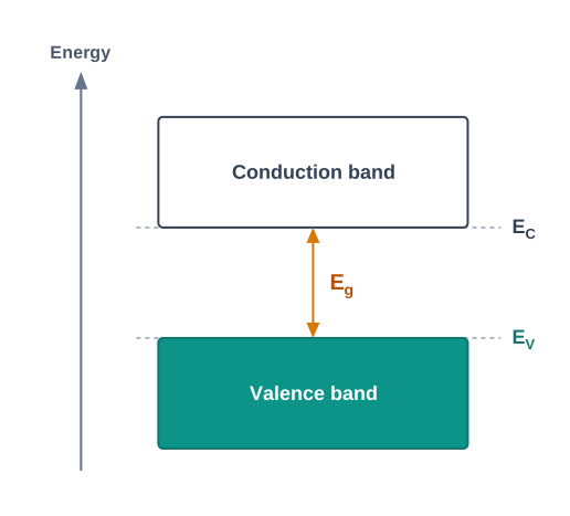
Fig. 14.1 – Energy bands of a semiconductor at absolute zero.
The lowest energy level of the conduction band is labelled \(E_C\), and the highest energy level of the valence band is labelled \(E_V\). Above \(E_C\) and below \(E_V\) there are very many closely spaced levels, as indicated in Fig. 14.1.
The gap between the top of the valence band (\(E_V\)) and the bottom of the conduction band (\(E_C\)) is called the energy band gap, or simply the energy gap \(E_g\).
The size of this gap may be large, small, or even zero, depending on the material. These three different situations are shown in Fig. 14.2 and discussed below.
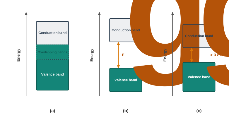
Fig. 14.2 – Energy bands in (a) metals, (b) insulators, and (c) semiconductors.
Case I — Metals [Fig. 14.2(a)]: A material behaves as a metal in either of two situations. In one, the conduction band is partially filled while the valence band is partially empty. In the other, the conduction and valence bands overlap. When there is overlap, electrons from the valence band can move very easily into the conduction band, making a large number of electrons available for conduction. And when the valence band is only partially empty, electrons in its lower levels can move up to higher levels, again allowing conduction. In both cases the resistance of the material is low, or equivalently its conductivity is high.
Case II — Insulators [Fig. 14.2(b)]: Here a large band gap exists, with \(E_g > 3\ \text{eV}\). There are no electrons in the conduction band, so no electrical conduction is possible. The gap is so large that ordinary thermal energy at room temperature cannot lift electrons from the valence band into the conduction band. This is the situation for insulators.
Case III — Semiconductors [Fig. 14.2(c)]: Here a finite but small band gap exists, with \(E_g < 3\ \text{eV}\). Because the gap is small, at room temperature some electrons from the valence band can gain just enough thermal energy to cross the gap and enter the conduction band. Although these electrons are few in number, they can move in the conduction band and carry current. This is why the resistance of a semiconductor is not as high as that of an insulator.
Thus, the width of the energy band gap is what fundamentally distinguishes a metal (bands overlap, \(E_g \approx 0\)), a semiconductor (small gap), and an insulator (large gap). This band picture, together with the resistivity ranges given earlier, is what decides whether a given solid conducts like a metal, blocks like an insulator, or behaves as a semiconductor.
In this section we have made a broad classification of metals, conductors, and semiconductors, both by their conductivity and by their energy bands. In the section that follows, we shall study how conduction actually takes place inside a semiconductor.
14.3 Intrinsic Semiconductor
A pure semiconductor, with no impurity added to it, is called an intrinsic semiconductor. To understand how such a pure crystal conduct electricity, we take the two most common examples, germanium (Ge) and silicon (Si).
The lattice structure of Si and Ge is shown in Fig. 14.3. It is called a diamond-like structure, because it is the same arrangement carbon atoms take in diamond. In this structure each atom is surrounded by four nearest neighbours, arranged symmetrically around it. The lattice spacing \(a\) (the repeat distance of the structure) is about 3.56 Å for carbon, 5.43 Å for silicon, and 5.66 Å for germanium.
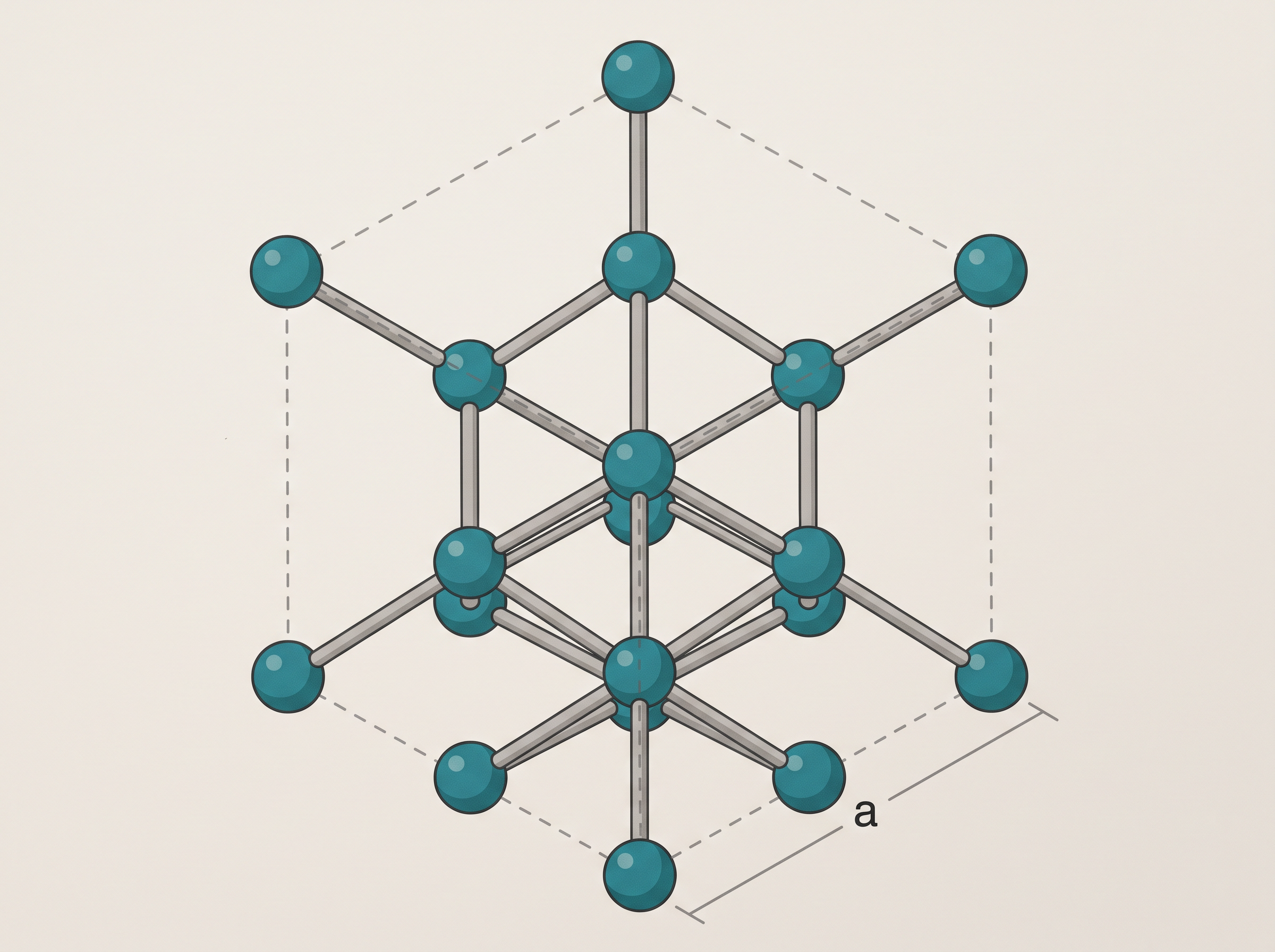
Fig. 14.3 – Diamond-like crystal structure of silicon and germanium.
Both Si and Ge have four valence electrons, that is, four electrons in their outermost orbit. In the crystal, every Si or Ge atom tends to share one of its four valence electrons with each of its four nearest neighbours, and in return to take a share of one electron from each of those neighbours. Each such shared pair of electrons forms what is called a covalent bond, or simply a valence bond. The two shared electrons can be pictured as shuttling back and forth between the two atoms they link, and this shared pair holds the two atoms together strongly.
Figure 14.4 shows a two-dimensional representation of this structure, drawn so as to emphasise the covalent bonds. It is an idealised picture in which no bond is broken — every bond is intact. Such a perfect, fully bonded situation occurs only at very low temperatures.
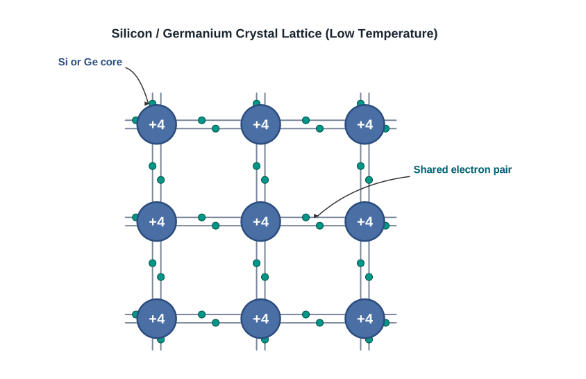
Fig. 14.4 – Two-dimensional schematic of the Si or Ge lattice.
As the temperature is raised, more thermal energy becomes available to the shared electrons. Some of them may then gain enough energy to break away from their bonds and become free electrons, which are then able to contribute to conduction. At any moderate temperature, this thermal energy manages to free the electrons of only a few atoms in the whole lattice.
When such an electron breaks free, it leaves an empty space in the bond it has left behind, as shown in Fig. 14.5(a). The neighbourhood from which the free electron (carrying charge \(-q\)) has departed is now short of one electron, so it is left with an effective charge of \(+q\). This vacancy, carrying an effective positive electronic charge, is called a hole. The hole behaves like an apparent free particle carrying a positive charge.
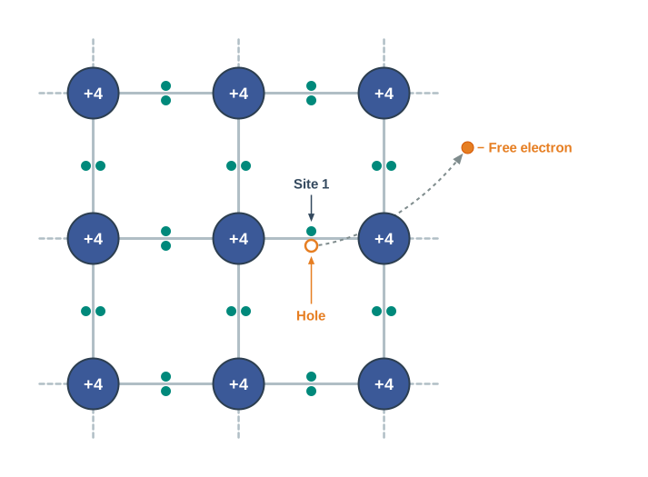
Fig. 14.5(a) – Generation of an electron-hole pair.
Because the crystal is pure, every electron that breaks free creates exactly one hole. So in an intrinsic semiconductor, the number of free electrons \(n_e\) is equal to the number of holes \(n_h\):
\[n_e = n_h = n_i \tag{14.1}\]
Here \(n_i\) is called the intrinsic carrier concentration, the number of free electrons (or of holes) per unit volume in the pure material at a given temperature. Its SI unit is \(\text{m}^{-3}\). Since more electrons break free as the crystal is heated, \(n_i\) increases with temperature.
Semiconductors have a special property that sets them apart: besides the free electrons, the holes also move and carry current. Let us see how a hole moves. Suppose there is a hole at a bond, which we call site 1, as shown in Fig. 14.5(a). An electron from a neighbouring covalent bond, at site 2, may jump across into the empty site 1. After this jump, site 1 is filled and the vacancy — the hole — is now at site 2, as shown in Fig. 14.5(b). Apparently, then, the hole has moved from site 1 to site 2.
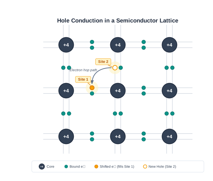
Fig. 14.5(b) – Apparent motion of a hole in the lattice.
It is important to note that the electron originally set free in Fig. 14.5(a) plays no part in this hole motion. That free electron moves entirely on its own as a conduction electron, and under an applied electric field it gives rise to an electron current \(I_e\). The motion of a hole, on the other hand, is only a convenient way of describing the actual motion of the bound electrons that keep hopping into whichever bond is currently empty.
Under an applied electric field, the holes drift towards the negative potential (opposite to the direction in which electrons move), giving a hole current \(I_h\). The total current \(I\) through an intrinsic semiconductor is therefore the sum of the electron current and the hole current:
\[I = I_e + I_h \tag{14.2}\]
where \(I_e\) is the current due to free electrons and \(I_h\) is the current due to holes, both measured in ampere (A).
The freeing of electrons is not the whole story. Alongside this generation of conduction electrons and holes, an opposite recombination process also goes on continuously, in which a free electron meets and fills a hole, so that both disappear together. At equilibrium, the rate of generation of charge carriers is exactly equal to the rate of recombination, so the number of carriers stays steady. This recombination happens when an electron collides with a hole.
We can now express all this in the band picture developed in the previous section. At \(T = 0\ \text{K}\), no bonds are broken, the conduction band is completely empty, and the intrinsic semiconductor behaves like an insulator, as shown in Fig. 14.6(a). It is only the thermal energy available at higher temperatures (\(T > 0\ \text{K}\)) that excites some electrons from the valence band up into the conduction band. These thermally excited electrons partly fill the conduction band, while leaving behind an equal number of holes in the valence band. The energy-band diagram of an intrinsic semiconductor at \(T > 0\ \text{K}\) is therefore as shown in Fig. 14.6(b).
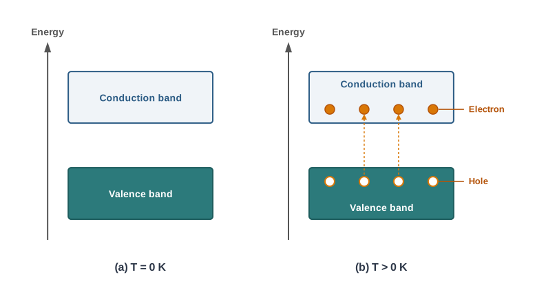
Fig. 14.6 – Energy band diagrams of an intrinsic semiconductor.
14.4 Extrinsic Semiconductor
The conductivity of an intrinsic (pure) semiconductor depends on its temperature, but at ordinary room temperature this conductivity is very low, because only a few electrons manage to break free. Such a weakly conducting material is not useful for building practical electronic devices. We therefore need a way to boost its conductivity in a controlled manner. This is done by deliberately adding impurities.
When a very small amount of a suitable impurity — say a few parts per million (ppm) — is added to a pure semiconductor, its conductivity increases manifold. A material treated in this way is called an extrinsic semiconductor, or an impurity semiconductor. The deliberate addition of a chosen impurity is called doping, the impurity atoms added are called dopants, and the resulting material is a doped semiconductor.
For doping to work well, the dopant must not disturb the original crystal lattice. It should occupy only a very few of the original semiconductor atom sites, slipping into the lattice without distorting it. A necessary condition for this is that the dopant atoms and the semiconductor atoms should be of nearly the same size.
Silicon and germanium are tetravalent (four valence electrons) and belong to the fourth group of the periodic table. So the dopant is chosen from a neighbouring group — the fifth group or the third group — so that its atomic size is close to that of Si or Ge. There are accordingly two types of dopants:
- (i) Pentavalent dopants (valency 5): such as arsenic (As), antimony (Sb), and phosphorus (P).
- (ii) Trivalent dopants (valency 3): such as indium (In), boron (B), and aluminium (Al).
Interestingly, these two kinds of dopants give two entirely different types of semiconductors, as discussed below.
(i) n-type semiconductor
Suppose we dope Si or Ge with a pentavalent element, as shown in Fig. 14.7. When an atom of valency 5 takes the place of a Si atom in the lattice, four of its five valence electrons form covalent bonds with the four neighbouring Si atoms. The fifth electron, however, is left over — it has no bond to join, and it remains only very weakly bound to its parent atom.
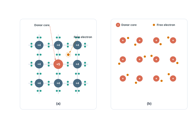
Fig. 14.7 – An n-type semiconductor and its fixed donor cores.
The reason the fifth electron is so loosely held is that the other four electrons, busy in bonding, are seen by it as part of the effective core of the atom. As a result, the ionisation energy needed to set this fifth electron free is very small, and even at room temperature it becomes free to move about in the lattice. The energy required is only about 0.01 eV for germanium and about 0.05 eV for silicon.
Compare this with the much larger energy needed to lift an ordinary bonded electron across the forbidden band (the energy gap) — about 0.72 eV for germanium and about 1.1 eV for silicon at room temperature in the intrinsic material. Clearly, the fifth electron of the pentavalent atom is freed far more easily than a normal bound electron.
Because the pentavalent dopant thus donates one extra electron for conduction, it is called a donor impurity.
The number of extra electrons made available by the dopant depends strongly on the doping level, and is essentially independent of any rise in the surrounding temperature. By contrast, the free electrons (and the equal number of holes) generated by the Si atoms themselves increase only weakly with temperature. So once doped, the dopant contribution dominates and does not change much with temperature.
In such a doped semiconductor, the total number of conduction electrons \(n_e\) is the sum of the electrons contributed by the donors and those generated intrinsically. The total number of holes \(n_h\), however, comes only from the intrinsic source. Moreover, because there are now so many more electrons around, the rate at which holes recombine with electrons increases, so the number of holes is reduced still further.
Thus, with a proper level of doping, the number of conduction electrons can be made much larger than the number of holes. In a semiconductor doped with a pentavalent impurity, electrons therefore become the majority carriers and holes the minority carriers. Such a material is called an n-type semiconductor (the “n” standing for the negative charge of the majority carriers). For an n-type semiconductor,
\[n_e \gg n_h \tag{14.3}\]
where \(n_e\) is the number of free electrons per unit volume and \(n_h\) the number of holes per unit volume.
(ii) p-type semiconductor
A p-type semiconductor is obtained when Si or Ge is doped with a trivalent impurity such as Al, B, or In. Such a dopant has one valence electron less than Si or Ge. It can form covalent bonds with only three of its four neighbouring Si atoms; it has no electron to offer to the fourth Si neighbour. So the bond between the trivalent atom and its fourth neighbour is left with a vacancy, that is, a hole, as shown in Fig. 14.8.
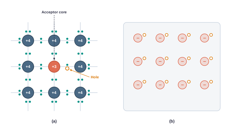
Fig. 14.8 – A p-type semiconductor and its fixed acceptor cores.
Since the neighbouring Si atom would prefer an electron in that empty position, an electron from the outer orbit of some nearby atom may jump in to fill this vacancy — but in doing so, it leaves a fresh vacancy (hole) at its own former site. In this way the hole is passed along and is available for conduction.
Note that when the trivalent atom accepts this extra electron to complete its fourth bond, it becomes effectively negatively charged. So the p-type dopant atom can be pictured as a fixed core carrying one negative charge, together with its associated hole, as shown in Fig. 14.8(b). Clearly, each such acceptor atom gives rise to one hole. These holes are in addition to the holes generated intrinsically, while the conduction electrons still come only from intrinsic generation.
For such a material, holes are therefore the majority carriers and electrons are the minority carriers. An extrinsic semiconductor doped with a trivalent impurity is called a p-type semiconductor (the “p” standing for the positive charge of the majority carriers). Here the recombination process reduces the number of intrinsically generated electrons to a smaller value \(n_e\). For a p-type semiconductor,
\[n_h \gg n_e \tag{14.4}\]
It is important to note that the crystal as a whole still remains electrically neutral. The charge of the additional mobile carriers is exactly balanced by the equal and opposite charge of the fixed, ionised dopant cores in the lattice.
In an extrinsic semiconductor, the majority carriers are so abundant that the few minority carriers produced thermally are very likely to meet a majority carrier and recombine (get destroyed). So, by flooding the crystal with carriers of one type, the dopant indirectly reduces the concentration of the minority carriers of the other type.
Doping also changes the energy-band structure. In an extrinsic semiconductor, additional allowed energy states appear because of the dopants: a donor level \(E_D\) due to donor impurities, and an acceptor level \(E_A\) due to acceptor impurities.
In the energy-band diagram of an n-type Si semiconductor, the donor level \(E_D\) lies just slightly below the bottom \(E_C\) of the conduction band, as shown in Fig. 14.9(a). Electrons sitting at this level need only a very small amount of energy to move up into the conduction band. At room temperature, almost all the donor atoms get ionised in this way, while only very few (of the order of \(10^{12}\) per cubic metre) Si atoms themselves get ionised. So the conduction band is filled mainly with electrons coming from the donor impurities.
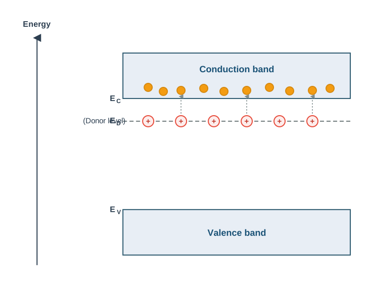
Fig. 14.9(a) – Energy bands of an n-type semiconductor.
Similarly, in a p-type semiconductor, the acceptor level \(E_A\) lies just slightly above the top \(E_V\) of the valence band, as shown in Fig. 14.9(b). With a very small supply of energy, an electron from the valence band can jump up to the level \(E_A\), ionising the acceptor negatively. (Equivalently, one may say that a hole from the level \(E_A\) sinks down into the valence band — electrons rise up and holes fall down when they gain external energy.) At room temperature, most acceptor atoms get ionised, leaving holes in the valence band. So at room temperature the density of holes in the valence band is predominantly due to the impurity, not the intrinsic material.
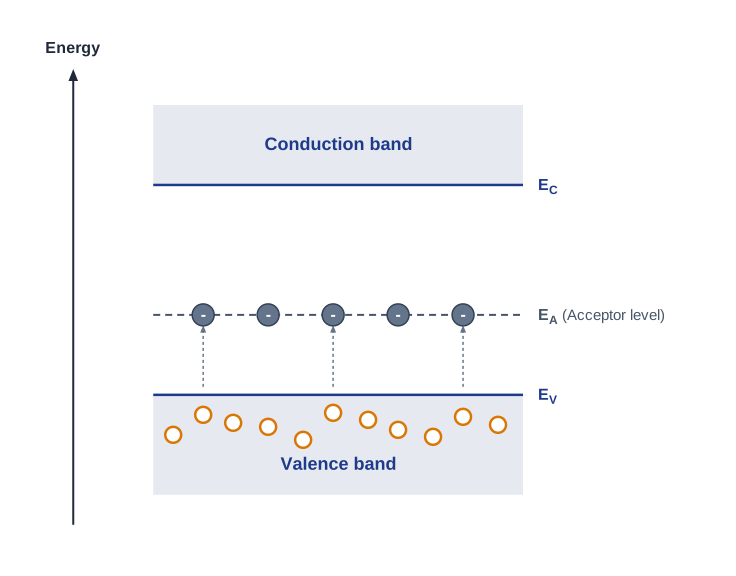
Fig. 14.9(b) – Energy bands of a p-type semiconductor.
The electron and hole concentrations in a semiconductor in thermal equilibrium are related by
\[n_e\, n_h = n_i^{\,2} \tag{14.5}\]
where \(n_e\) and \(n_h\) are the electron and hole concentrations (in \(\text{m}^{-3}\)) and \(n_i\) is the intrinsic carrier concentration. This important relation holds for intrinsic as well as extrinsic (both n-type and p-type) semiconductors, and shows that increasing the majority carriers automatically decreases the minority carriers.
Although this whole description is only a rough and simplified picture, it helps us understand, in a simple way, the difference between metals, insulators, and semiconductors (both intrinsic and extrinsic). The difference in the resistivity of C, Si, and Ge comes from the difference in the energy gap between their conduction and valence bands. For carbon (diamond), silicon, and germanium, the energy gaps are 5.4 eV, 1.1 eV, and 0.7 eV respectively. Tin (Sn) is also a group IV element, but it behaves as a metal because its energy gap is 0 eV.
14.5 p-n Junction
A p-n junction is the basic building block of many semiconductor devices, such as diodes and transistors. Understanding how such a junction behaves is essential, because the working of most other semiconductor devices depends on it. In this section we shall see how a p-n junction is formed, and later how it behaves when an external voltage — also called a bias — is applied across it.
14.5.1 p-n junction formation
Consider a thin wafer of p-type silicon (p-Si). By adding a precisely controlled small quantity of a pentavalent impurity to a part of this wafer, that part can be converted into n-type silicon (n-Si). (There are several technical processes by which this can be done.) The wafer now contains a p-region and an n-region, with a boundary between them known as the metallurgical junction.
Two important processes take place during the formation of a p-n junction: diffusion and drift.
Recall that in an n-type semiconductor the concentration of electrons is much greater than that of holes, while in a p-type semiconductor the concentration of holes is much greater than that of electrons. So across the junction there is a steep difference in concentration — a concentration gradient — for both types of carriers.
Just as a gas spreads from a region where it is dense to a region where it is sparse, charge carriers move from where they are plentiful to where they are scarce. Because of this concentration gradient, holes diffuse from the p-side to the n-side (\(p \rightarrow n\)), and electrons diffuse from the n-side to the p-side (\(n \rightarrow p\)). This motion of charge carriers due to the concentration gradient gives rise to a diffusion current across the junction.
Now consider what these diffusing carriers leave behind. When an electron diffuses from the n-side to the p-side, it leaves behind, on the n-side, an ionised donor atom carrying a positive charge. This ionised donor is immobile, because it is firmly bonded to the surrounding atoms and cannot move. As more and more electrons diffuse away from the n-side, a layer of positive charge — a positive space-charge region — builds up on the n-side of the junction.
Similarly, when a hole diffuses from the p-side to the n-side, it leaves behind, on the p-side, an ionised acceptor atom carrying a negative charge, which is also immobile. As more holes diffuse away, a layer of negative charge — a negative space-charge region — builds up on the p-side of the junction.
Together, these two space-charge layers on either side of the junction form the depletion region. It is given this name because the diffusing electrons and holes have “depleted” this region of its free charge carriers, leaving behind only the fixed, ionised cores, as shown in Fig. 14.10. The depletion region is extremely thin — its thickness is of the order of one-tenth of a micrometre (\(\sim 0.1\ \mu\text{m}\)).
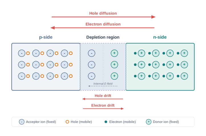
Fig. 14.10 – Formation of a p-n junction and the depletion region.
Because there is now a positive space-charge region on the n-side and a negative space-charge region on the p-side, an electric field develops across the depletion region, directed from the positive charge towards the negative charge (that is, from the n-side to the p-side). This built-in field pushes any electron that happens to be on the p-side back towards the n-side, and any hole on the n-side towards the p-side. The motion of charge carriers caused by this electric field is called drift, and it constitutes a drift current, which flows in the direction opposite to the diffusion current (Fig. 14.10).
Initially, the diffusion current is large and the drift current is small. But as diffusion continues, the space-charge regions on either side keep extending, which strengthens the electric field and hence increases the drift current. This process goes on until the drift current becomes just equal to the diffusion current. At that point the p-n junction is fully formed, and in a p-n junction under equilibrium there is no net current.
The diffusion of carriers also produces a difference of potential across the junction. The n-region has lost electrons (and gained fixed positive ions), while the p-region has gained electrons (and fixed negative ions). As a result, the n-material becomes positive relative to the p-material. Figure 14.11 shows this p-n junction at equilibrium, together with the potential across the junction.
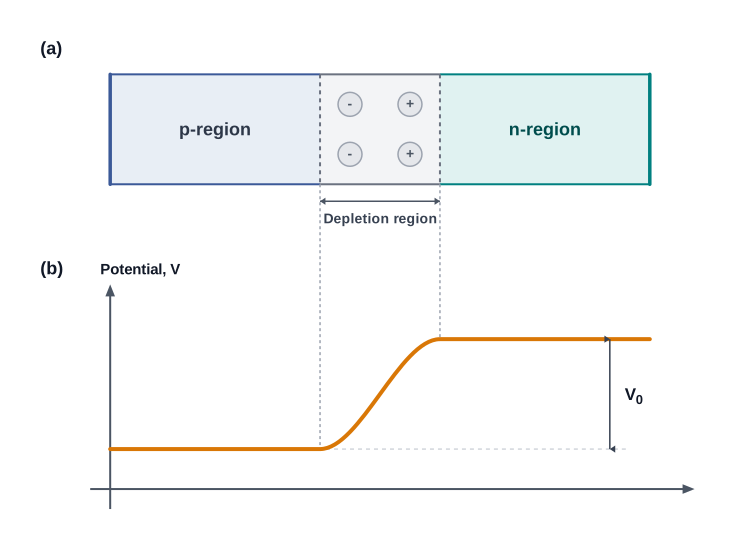
Fig. 14.11 – p-n junction at equilibrium and its barrier potential.
The polarity of this potential is such that it opposes any further flow of carriers, which is exactly what keeps the junction in equilibrium. Because this potential tends to prevent electrons from moving from the n-region into the p-region, it is called the barrier potential \(V_0\).
14.6 Semiconductor Diode
A semiconductor diode is basically a p-n junction with metallic contacts provided at its two ends, so that an external voltage can be applied across it, as shown in Fig. 14.12(a). It is therefore a two-terminal device. The symbol used for a p-n junction diode is shown in Fig. 14.12(b).
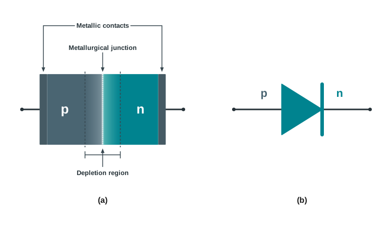
Fig. 14.12 – Semiconductor diode and its circuit symbol.
In the diode symbol, the arrow points from the p-side to the n-side and indicates the conventional direction of current flow when the diode is forward biased. As we saw in the previous section, at equilibrium the junction has a built-in barrier potential \(V_0\). This barrier can be altered by applying an external voltage \(V\) across the diode. The equilibrium situation (with no external voltage, \(V = 0\)) was shown in Fig. 14.11. We now study what happens when a voltage is applied in each of the two possible directions.
14.6.1 p-n junction diode under forward bias
When an external voltage \(V\) is applied across the diode such that the p-side is connected to the positive terminal of the battery and the n-side to the negative terminal [Fig. 14.13(a)], the diode is said to be forward biased.
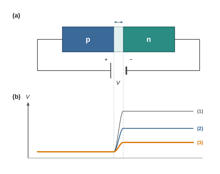
Fig. 14.13 – p-n junction diode under forward bias.
The applied voltage appears almost entirely across the depletion region, and the voltage drop across the p-side and n-side of the junction is negligible. This is because the depletion region — having almost no free charges — has a very high resistance compared with the resistance of the n-side and p-side. The direction of the applied voltage \(V\) is opposite to that of the built-in potential \(V_0\). As a result, the depletion layer width decreases and the barrier height is reduced [Fig. 14.13(b)]. The effective barrier height under forward bias becomes
\[V_{\text{eff}} = (V_0 - V).\]
If the applied voltage is small, the barrier is lowered only slightly below its equilibrium value. Then only a small number of carriers — those in the highest energy levels — have enough energy to cross the junction, so the current is small. If we increase the applied voltage significantly, the barrier height is reduced much more, so many more carriers acquire enough energy to cross. Thus the current increases.
Because of the applied voltage, electrons from the n-side cross the depletion region and reach the p-side, where they are now the minority carriers. Likewise, holes from the p-side cross the junction and reach the n-side, where they too are minority carriers. This process under forward bias is called minority carrier injection. At the junction boundary, on each side, the minority carrier concentration rises sharply compared with its value far from the junction.
Owing to this concentration gradient, the injected electrons on the p-side diffuse from the junction edge towards the far end of the p-side, and the injected holes on the n-side diffuse from the junction edge towards the far end of the n-side, as shown in Fig. 14.14. This motion of the injected charge carriers on both sides constitutes the current. The total forward current is the sum of the hole diffusion current and the conventional current due to electron diffusion. Its magnitude is usually of the order of milliamperes (mA).
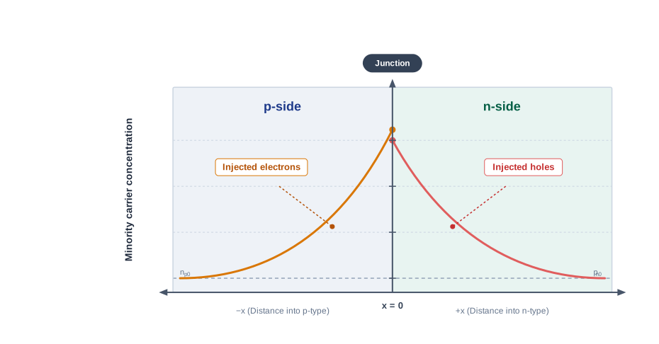
Fig. 14.14 – Minority carrier injection under forward bias.
14.6.2 p-n junction diode under reverse bias
When an external voltage \(V\) is applied across the diode such that the n-side is connected to the positive terminal and the p-side to the negative terminal, the diode is said to be reverse biased [Fig. 14.15(a)].
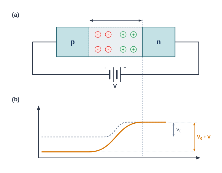
Fig. 14.15 – p-n junction diode under reverse bias.
Here again the applied voltage appears mostly across the depletion region. But now the direction of the applied voltage is the same as that of the barrier potential. As a result, the barrier height increases and the depletion region widens, because of the change in the electric field. The effective barrier height under reverse bias becomes
\[V_{\text{eff}} = (V_0 + V),\]
as shown in Fig. 14.15(b). This raised barrier strongly suppresses the flow of electrons from \(n \rightarrow p\) and of holes from \(p \rightarrow n\). So the diffusion current decreases enormously compared with the forward-biased diode.
However, a small current still flows. The electric field of the junction is such that if a minority electron on the p-side, or a minority hole on the n-side, happens to wander close to the junction in its random motion, it is quickly swept across to the other side. This drift of minority carriers gives rise to a small current, of the order of a few microamperes (\(\mu\text{A}\)). It is small because it depends only on the few minority carriers crossing from their minority side to their majority side. (A tiny drift current also exists under forward bias, but there it is negligible — μA — compared with the mA current due to injected carriers.)
An important point is that this reverse current does not depend much on the applied voltage. Even a small reverse voltage is enough to sweep across all the available minority carriers. So the current is limited not by the applied voltage but by the concentration of minority carriers on either side of the junction.
This behaviour holds up to a certain critical reverse voltage called the breakdown voltage (\(V_{br}\)). When \(V = V_{br}\), the reverse current increases sharply, and even a slight further increase in voltage causes a large change in current. If this reverse current is not limited by an external circuit to below the rated value specified by the manufacturer, the p-n junction gets destroyed by overheating. (The same destruction can happen even under forward bias if the forward current exceeds the rated value.) This special breakdown action of the diode is put to use in special-purpose diodes.
V–I characteristics. To study how the current varies with the applied voltage — the V–I characteristics of the diode — the circuit arrangements of Fig. 14.16(a) and (b) are used. The battery is connected to the diode through a potentiometer (or rheostat) so that the voltage applied to the diode can be varied. For different voltages, the current is noted, and a graph of \(V\) against \(I\) is plotted, as in Fig. 14.16(c). In forward bias the expected current is large, so a milliammeter is used; in reverse bias the current is very small, so a microammeter is used.
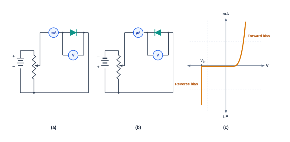
Fig. 14.16 – Circuit arrangements and V–I characteristics of a diode.
In forward bias, the current first increases very slowly, almost negligibly, until the voltage across the diode crosses a certain value. After this characteristic voltage, the current increases rapidly (exponentially), even for a very small further increase in voltage. This voltage is called the threshold voltage or cut-in voltage (about 0.2 V for a germanium diode and about 0.7 V for a silicon diode).
In reverse bias, the current is very small (\(\sim \mu\text{A}\)) and remains almost constant as the bias is changed. This is called the reverse saturation current. Only at very high reverse bias (the breakdown voltage) does the current suddenly increase. General-purpose diodes are not used beyond the reverse saturation current region.
The above discussion shows that a p-n junction diode primarily allows current to flow only in one direction — the forward direction. Its forward-bias resistance is low, while its reverse-bias resistance is high. This one-way property is exactly what is used to rectify alternating voltages, as discussed in the next section.
For diodes, we define a quantity called the dynamic resistance \(r_d\) as the ratio of a small change in voltage \(\Delta V\) to the corresponding small change in current \(\Delta I\):
\[r_d = \frac{\Delta V}{\Delta I} \tag{14.6}\]
Here \(\Delta V\) is in volt (V) and \(\Delta I\) in ampere (A), so \(r_d\) is in ohm (\(\Omega\)). Because the V–I graph is a curve (not a straight line), the diode’s resistance is not constant, so this dynamic (small-change) resistance is used to describe its behaviour at a chosen operating point.
The V–I characteristic of a silicon diode is shown in Fig. 14.17. Calculate the resistance of the diode at (a) a forward current \(I_D = 15\ \text{mA}\), and (b) a reverse voltage \(V_D = -10\ \text{V}\).
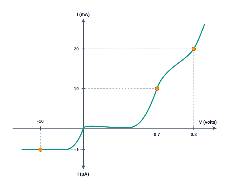
[Caption:] Fig. 14.17 – V–I characteristic with operating points marked. [/Caption:]
Solution: We treat the diode’s forward characteristic between \(I = 10\ \text{mA}\) and \(I = 20\ \text{mA}\) as a straight line passing through the origin, and use Ohm’s law to find the resistance.
- From the curve, at \(I = 20\ \text{mA}\), \(V = 0.8\ \text{V}\); and at \(I = 10\ \text{mA}\), \(V = 0.7\ \text{V}\). The forward-bias resistance is
\[r_{fb} = \frac{\Delta V}{\Delta I} = \frac{0.1\ \text{V}}{10\ \text{mA}} = 10\ \Omega.\]
- From the curve, at \(V = -10\ \text{V}\), \(I = -1\ \mu\text{A}\). The reverse-bias resistance is
\[r_{rb} = \frac{10\ \text{V}}{1\ \mu\text{A}} = 1.0 \times 10^{7}\ \Omega.\]
The huge difference between \(r_{fb} = 10\ \Omega\) and \(r_{rb} = 1.0 \times 10^{7}\ \Omega\) shows clearly why the diode conducts easily in the forward direction but almost blocks current in the reverse direction.
14.7 Application of Junction Diode as a Rectifier
From the V–I characteristic of a junction diode, we know that it allows current to pass only when it is forward biased. So if an alternating voltage is applied across a diode, current flows only during that part of each cycle in which the diode is forward biased. This one-way property is used to rectify alternating voltages — that is, to convert alternating current (ac) into direct current (dc) — and the circuit used for this purpose is called a rectifier.
Half-wave rectifier
Suppose an alternating voltage is applied across a diode connected in series with a load. Then a pulsating voltage appears across the load only during those half cycles of the ac input in which the diode is forward biased. Such a circuit, shown in Fig. 14.18, is called a half-wave rectifier.
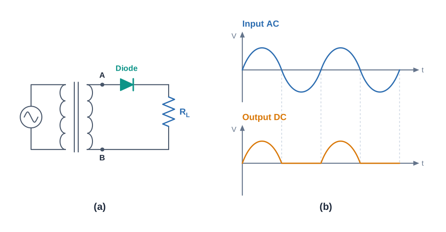
Fig. 14.18 – Half-wave rectifier circuit and waveforms.
The secondary coil of a transformer supplies the required ac voltage across the terminals A and B. When the voltage at A is positive, the diode is forward biased and conducts. When the voltage at A is negative, the diode is reverse biased and does not conduct. The reverse saturation current of the diode is negligible and can be taken as zero for practical purposes. (The reverse breakdown voltage of the diode must be kept sufficiently higher than the peak ac voltage at the transformer secondary, to protect the diode from reverse breakdown.)
Therefore, during the positive half-cycle of the ac, there is a current through the load resistor \(R_L\) and we obtain an output voltage, as shown in Fig. 14.18(b). During the negative half-cycle there is no current, so there is no output. In the next positive half-cycle, we again get an output voltage. Thus the output voltage, though still varying, is restricted to only one direction, and is said to be rectified. Since this circuit gives a rectified output for only half of each input ac wave, it is called a half-wave rectifier.
This is the essential idea behind turning ac into dc: the junction’s one-way conduction blocks one half of every ac cycle, leaving an output that flows in a single direction. A full-wave circuit and a filter (described below) then improve this into a steady dc voltage.
Full-wave rectifier
A circuit using two diodes, shown in Fig. 14.19(a), gives a rectified output corresponding to both the positive and the negative halves of the ac cycle. It is therefore called a full-wave rectifier.
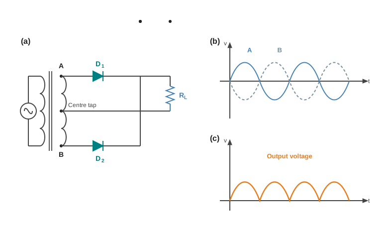
Fig. 14.19 – Full-wave rectifier circuit and waveforms.
Here the p-sides of the two diodes are connected to the two ends of the transformer secondary, while their n-sides are joined together. The output is taken between this common point of the diodes and the midpoint of the transformer secondary. For this reason the secondary is provided with a centre tapping, and the transformer is called a centre-tap transformer. As seen in Fig. 14.19(c), the voltage rectified by each diode is only half the total secondary voltage. Each diode rectifies for only half the cycle, but the two of them do so during alternate half-cycles. (There is also another full-wave rectifier circuit that does not need a centre-tap transformer but instead uses four diodes.)
Let us follow one full cycle. Suppose that, at some instant, the voltage at A (measured with respect to the centre tap) is positive. Since the two ends of the secondary are out of phase, the voltage at B at that instant is negative, as shown in Fig. 14.19(b). So diode \(D_1\) is forward biased and conducts, while diode \(D_2\), being reverse biased, does not conduct. During this positive half-cycle we get an output current, and hence an output voltage across the load \(R_L\), as in Fig. 14.19(c).
In the next part of the ac cycle, the voltage at A becomes negative with respect to the centre tap, so the voltage at B becomes positive. Now \(D_1\) does not conduct but \(D_2\) does, again giving an output current and output voltage across \(R_L\), this time during the negative half-cycle of the input. Thus we obtain an output during both the positive and the negative halves of every cycle. Clearly, this is a more efficient way of obtaining rectified voltage or current than the half-wave rectifier.
Filter
The rectified voltage so far is in the form of pulses shaped like half sinusoids. Although it is unidirectional (dc in direction), it does not have a steady value — it keeps rising and falling. To obtain a steady dc output from this pulsating voltage, a capacitor is normally connected across the output terminals, in parallel with the load \(R_L\). (An inductor in series with \(R_L\) can also serve the same purpose.) Because these additional components appear to “filter out” the ac ripple and leave a purer dc voltage, they are called filters.
Let us see how the capacitor does this smoothing. When the rectified voltage across the capacitor is rising, the capacitor charges up. If there were no external load, it would simply stay charged to the peak voltage of the rectified output. When a load is present, the capacitor discharges through the load during the intervals when the rectified voltage falls, so the voltage across it begins to drop. Then, in the next half-cycle of the rectified output, it charges back up to the peak value, as shown in Fig. 14.20. The overall effect is an output that stays close to the peak value, with only a small ripple.
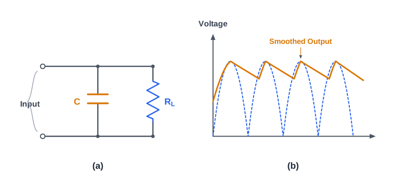
Fig. 14.20 – Full-wave rectifier with a capacitor filter.
The rate at which the capacitor voltage falls between charging pulses depends inversely on the product of the capacitance \(C\) and the effective resistance \(R_L\) in the circuit. This product is called the time constant of the circuit.
To make the time constant large, the value of \(C\) must be large. This is why capacitor-input filters use large capacitors. The output voltage obtained with such a capacitor-input filter is close to the peak voltage of the rectified waveform. This type of filter is the one most widely used in power supplies.
14.8 Summary
Semiconductors are the basic materials used in today’s solid-state electronic devices, such as diodes, transistors, and integrated circuits (ICs).
It is the lattice structure and the atomic structure of the constituent elements that decide whether a particular material behaves as an insulator, a metal, or a semiconductor.
Metals have low resistivity (\(10^{-2}\) to \(10^{-8}\ \Omega\,\text{m}\)) and insulators have very high resistivity (\(> 10^{8}\ \Omega\,\text{m}^{-1}\)), while semiconductors have resistivity values that lie in between these two.
Semiconductors may be elemental (Si, Ge) or compound (GaAs, CdS, etc.).
Pure semiconductors are called intrinsic semiconductors. In them, the presence of charge carriers (electrons and holes) is an intrinsic property of the material, produced by thermal excitation. The number of electrons (\(n_e\)) equals the number of holes (\(n_h\)). Holes are essentially electron vacancies that carry an effective positive charge.
The number of charge carriers can be changed by doping a pure semiconductor with a suitable impurity. Such materials are called extrinsic semiconductors, and they are of two types: n-type and p-type.
In n-type semiconductors, \(n_e \gg n_h\), while in p-type semiconductors, \(n_h \gg n_e\).
n-type Si or Ge is obtained by doping with pentavalent atoms (donors) such as As, Sb, P, while p-type Si or Ge is obtained by doping with trivalent atoms (acceptors) such as B, Al, In.
In all cases, \(n_e\, n_h = n_i^{\,2}\), and the material as a whole maintains overall electrical charge neutrality.
The electrons in a material occupy two distinct bands of energy — the valence band and the conduction band. Valence-band energies are lower than conduction-band energies. All the levels in the valence band are filled, while the levels in the conduction band may be completely empty or partially filled. The electrons in the conduction band are free to move through the solid and are responsible for its conductivity. The extent of conductivity depends on the energy gap (\(E_g\)) between the top of the valence band (\(E_V\)) and the bottom of the conduction band (\(E_C\)). Electrons from the valence band can be raised to the conduction band by supplying heat, light, or electrical energy, thereby changing the current in the semiconductor.
For insulators, \(E_g > 3\ \text{eV}\); for semiconductors, \(E_g\) lies between \(0.2\ \text{eV}\) and \(3\ \text{eV}\); and for metals, \(E_g \approx 0\).
The p-n junction is the key to all semiconductor devices. When such a junction is formed, a depletion layer is created, consisting of immobile ion-cores that have been stripped of their electrons or holes. This depletion layer is responsible for the junction potential barrier.
By changing the external applied voltage, the junction barrier can be altered. In forward bias (n-side connected to the negative terminal and p-side to the positive terminal of the battery), the barrier is decreased, whereas in reverse bias the barrier is increased. Hence the forward-bias current is large (in mA), while the reverse-bias current is very small (in \(\mu\)A) in a p-n junction diode.
Diodes can be used to rectify an ac voltage (restricting the current to one direction). With the help of a capacitor or a suitable filter, a steady dc voltage can then be obtained.
14.9 Points to Ponder
The energy bands, marked by \(E_C\) and \(E_V\), are space-delocalised in a semiconductor. This means they are not tied to any particular location inside the solid — the energies they stand for are overall averages taken across the whole crystal. So when you see a diagram in which \(E_C\) or \(E_V\) is drawn as a single straight line, you should read that line simply as the bottom of the conduction-band energy levels (\(E_C\)) or the top of the valence-band energy levels (\(E_V\)), and not as an energy belonging to one fixed spot in the material.
In elemental semiconductors (Si or Ge), an n-type or p-type semiconductor is produced by deliberately introducing dopants, which act as defects in the crystal. In compound semiconductors, the type of semiconductor can also be changed by altering the relative stoichiometric ratio of the elements. For example, in ideal gallium arsenide the ratio of Ga to As is 1:1, but in Ga-rich or As-rich GaAs it could be \(\text{Ga}_{1.1}\text{As}_{0.9}\) or \(\text{Ga}_{0.9}\text{As}_{1.1}\) respectively. In general, the presence of defects controls the properties of semiconductors in many different ways.
14.10 NCERT Questions
In an n-type silicon, which of the following statements is true:
- Electrons are majority carriers and trivalent atoms are the dopants.
- Electrons are minority carriers and pentavalent atoms are the dopants.
- Holes are minority carriers and pentavalent atoms are the dopants.
- Holes are majority carriers and trivalent atoms are the dopants.
Which of the statements given in Question 1 is true for a p-type semiconductor?
Carbon, silicon, and germanium have four valence electrons each. They are characterised by valence and conduction bands separated by an energy band gap equal to \((E_g)_{\text{C}}\), \((E_g)_{\text{Si}}\), and \((E_g)_{\text{Ge}}\) respectively. Which of the following statements is true?
- \((E_g)_{\text{Si}} < (E_g)_{\text{Ge}} < (E_g)_{\text{C}}\)
- $(E_g){} < (E_g){} > \((E_g)_{\text{Si}}\)
- \((E_g)_{\text{C}} > (E_g)_{\text{Si}} > (E_g)_{\text{Ge}}\)
- \((E_g)_{\text{C}} = (E_g)_{\text{Si}} = (E_g)_{\text{Ge}}\)
In an unbiased p-n junction, holes diffuse from the p-region to the n-region because
- free electrons in the n-region attract them.
- they move across the junction by the potential difference.
- hole concentration in the p-region is more as compared to the n-region.
- All the above.
When a forward bias is applied to a p-n junction, it
- raises the potential barrier.
- reduces the majority carrier current to zero.
- lowers the potential barrier.
- None of the above.
In half-wave rectification, what is the output frequency if the input frequency is 50 Hz? What is the output frequency of a full-wave rectifier for the same input frequency?
14.11 Check Your Concepts
State four important advantages that solid-state semiconductor devices have over the older vacuum tubes (valves).
Using the idea of energy bands, explain how a conductor, an insulator, and a semiconductor differ from one another. In each case, comment on the size of the energy band gap.
What is meant by a “hole” in a semiconductor? Explain how the apparent motion of a hole actually corresponds to the motion of bound electrons in the crystal.
The conductivity of a pure semiconductor increases when it is heated, whereas the conductivity of a metal decreases on heating. Explain the reason for this difference in behaviour.
When a semiconductor is doped, a large number of extra charge carriers are introduced, yet the crystal remains electrically neutral. Explain why.
Distinguish between diffusion current and drift current during the formation of a p-n junction. Why is there no net current across the junction when it is in equilibrium?
Describe what happens to (i) the width of the depletion region and (ii) the height of the potential barrier when a p-n junction diode is (a) forward biased and (b) reverse biased.
It is observed that the current in a reverse-biased diode remains almost constant even when the reverse voltage is increased (up to breakdown). Give the reason for this behaviour.
Explain why a full-wave rectifier is more efficient than a half-wave rectifier. What is the function of the capacitor connected across the load in a rectifier circuit?
14.12 Practice with Numericals
A pure silicon sample is doped with a trivalent (acceptor) impurity so that the hole concentration becomes \(n_h = 4.5 \times 10^{22}\ \text{m}^{-3}\). If the intrinsic carrier concentration is \(n_i = 1.5 \times 10^{16}\ \text{m}^{-3}\), calculate the electron concentration \(n_e\), and state whether the sample is n-type or p-type.
A semiconductor sample has a resistivity of \(0.5\ \Omega\,\text{m}\) at a certain temperature. Calculate its electrical conductivity, and state its SI unit.
For a silicon diode, when the forward voltage is increased from \(0.65\ \text{V}\) to \(0.75\ \text{V}\), the forward current increases from \(4\ \text{mA}\) to \(24\ \text{mA}\). Calculate the dynamic resistance of the diode over this range.
A silicon wafer contains \(4 \times 10^{28}\) atoms \(\text{m}^{-3}\). It is doped with phosphorus at a concentration of 2 ppm (parts per million). Calculate the donor concentration \(N_D\) introduced by the doping.